NAME Gailu biomedikoak diseinatzeko eta fabrikatzeko ekipamendu eta laborategiak
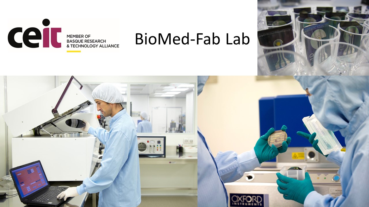
Aplikazio biomedikoetan erabiltzeko eta mikroteknologietan oinarritutako gailuen diseinu, fabrikazio eta karakterizazioa. Plataforma mikrofluidikoak, biosentsoreak eta mikroelektrodo funtzionalak, bai eta tarteko egiturak ere, hala nola erreplikatzeko edo estanpatzeko moldeak edo nanozuntz polimerikoko mintzak. Silizio, beira, alumina edo material polimerikoko (termoplastikoak eta elastomeroak) substratuak. Metal nobleen elektrodoak, silizio oxidoaren, silizio nitruroan edo erretxina estrukturalen pasibazio-geruzen bidez eremu aktiboak konfinatzeko aukera dutenak.
FIELDS OF APPLICATION
Additive manufacturing
Biomedical consumables
Electromedical devices
In-Vitro diagnostics
Laboratory equipment
MOST OUTSTANDING EQUIPMENT AND COMPONENTS
-
Double side insulator-aligner (EVG-620 model) and semi-automatic hot-embossing system (EVG-510 model)
Double side insulator-aligner (EVG-620 model) and semi-automatic hot-embossing system (EVG-510 model)
-
Electrospinning set-up for the fabrication of simple or coaxial polymeric nanofibers, with or without drug loading, in random or semi-ordered configuration according to pre-established patterns
Electrospinning set-up for the fabrication of simple or coaxial polymeric nanofibers, with or without drug loading, in random or semi-ordered configuration according to pre-established patterns
-
Equipment for vapor phase deposition of thin films (PECVD) and reactive etching system (RIE), PLASMALAB 80+ from OXFORD Instruments models
Equipment for vapor phase deposition of thin films (PECVD) and reactive etching system (RIE), PLASMALAB 80+ from OXFORD Instruments models
-
Programmable wafer cutter MICROACE SERIES 3 from LOAD POINT LTD
Programmable wafer cutter MICROACE SERIES 3 from LOAD POINT LTD
-
PVD thin film deposition system, Pfeiffer CLASSIC 500 model with four 2DC-1 PDC-1 RF magnetron cathodes and the possibility of high temperature deposition
PVD thin film deposition system, Pfeiffer CLASSIC 500 model with four 2DC-1 PDC-1 RF magnetron cathodes and the possibility of high temperature deposition
SERVICES OFFERED BY THE ASSET
3D microstructure replication
Fabrication of elastomeric mould replicas by casting or transferring of mould microstructures to thermoplastics by hot embossing techniques
Bonding of different materials
Reversible or irreversible bonding of silicon, glass and polymers by means of the corresponding technique: anodic bonding or surface activation by oxygen plasma
Bulk etching of silicon
Bulk removal of silicon by means of micromachining techniques
Device design
Personalised design of biosensors, polymeric membranes and microfluidic platforms
Fabrication of polymer nanofiber membranes
Fabrication of simple or coaxial polymer nanofibers either with or without drug load, in random or patterned configurations
hin film etching
Selective removal of thin films by means of wet and/or dry etching (RIE)
Mould fabrication (with 3D microstructures)
Structural photoresist-based moulds obtained by UV lithography or metal layer-based moulds by electroplating
Oxygen plasma treatments
Modification of surface properties (hydrophobicity or hydrophilicity) by means of oxygen plasma activation
Structure characterization
Measurement of the thickness from thin films (a few nm) up to 120 um-thick microstructures by profilometry and/or atomic force microscopy
Thermal annealing
Thermal annealing of devices in non-reactive environments up to 1200ºC
Thin film deposition
Deposition of up to 5µm-thick layers onto planar substrates (max. diameter 10 cm). Films can be made of metals, metal oxides or silicon oxides or nitrides, and deposited by PVD, CVD or electroplating techniques
UV photolithography
Resist patterning for microelectrode definition or passivation layer etching
Wafer dicing
Dicing of whole wafers of silicon, glass or thermoplastics into individualized devices with customized dimensions
ENTITY MANAGING THE ASSET
Contact person:
Sergio Arana
sarana@ceit.es