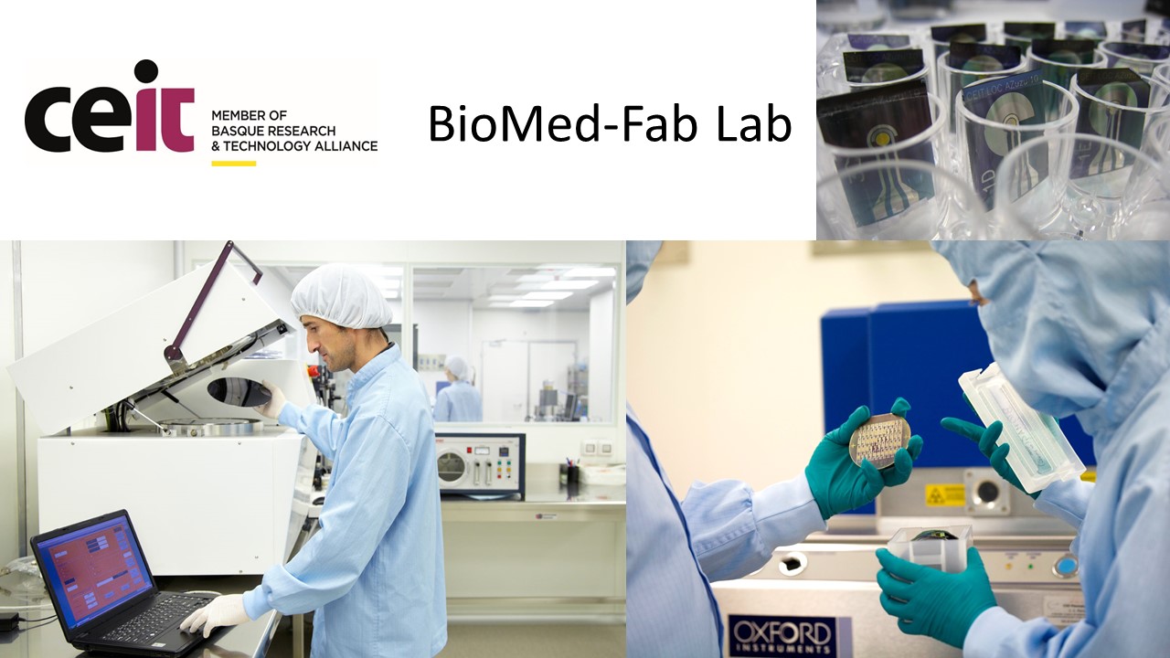
Laboratories and equipment to design and fabricate biomedical devices
DESCRIPTION
Design, fabrication and characterization of devices based on microtechnologies for their use in biomedical applications. Microfluidic platforms, biosensors and functional microelectrodes, as well as intermediate structures such as moulds for replication or stamping and polymeric nanofiber scaffolds. Silicon, glass, alumina or polymeric material (thermoplastics and elastomers) substrates. Noble metal electrodes with the possibility of confining active areas through passivation layers of silicon oxide, silicon nitride or structural resins.
MOST OUTSTANDING EQUIPMENT AND COMPONENTS
Double side insulator-aligner (EVG-620 model) and semi-automatic hot-embossing system (EVG-510 model)Double side insulator-aligner (EVG-620 model) and semi-automatic hot-embossing system (EVG-510 model)
Electrospinning set-up for the fabrication of simple or coaxial polymeric nanofibers, with or without drug loading, in random or semi-ordered configuration according to pre-established patterns
Equipment for vapor phase deposition of thin films (PECVD) and reactive etching system (RIE), PLASMALAB 80+ from OXFORD Instruments models
Programmable wafer cutter MICROACE SERIES 3 from LOAD POINT LTD
PVD thin film deposition system, Pfeiffer CLASSIC 500 model with four 2DC-1 PDC-1 RF magnetron cathodes and the possibility of high temperature deposition
SERVICES OFFERED BY THE ASSET

3D microstructure replication
Bonding of different materials
Bulk etching of silicon
Device design
Fabrication of polymer nanofiber membranes
hin film etching
Mould fabrication (with 3D microstructures)
Oxygen plasma treatments
Structure characterization
Thermal annealing
Thin film deposition
UV photolithography
Wafer dicing
ENTITY MANAGING THE ASSET
CEIT
Contact person: Sergio Arana


